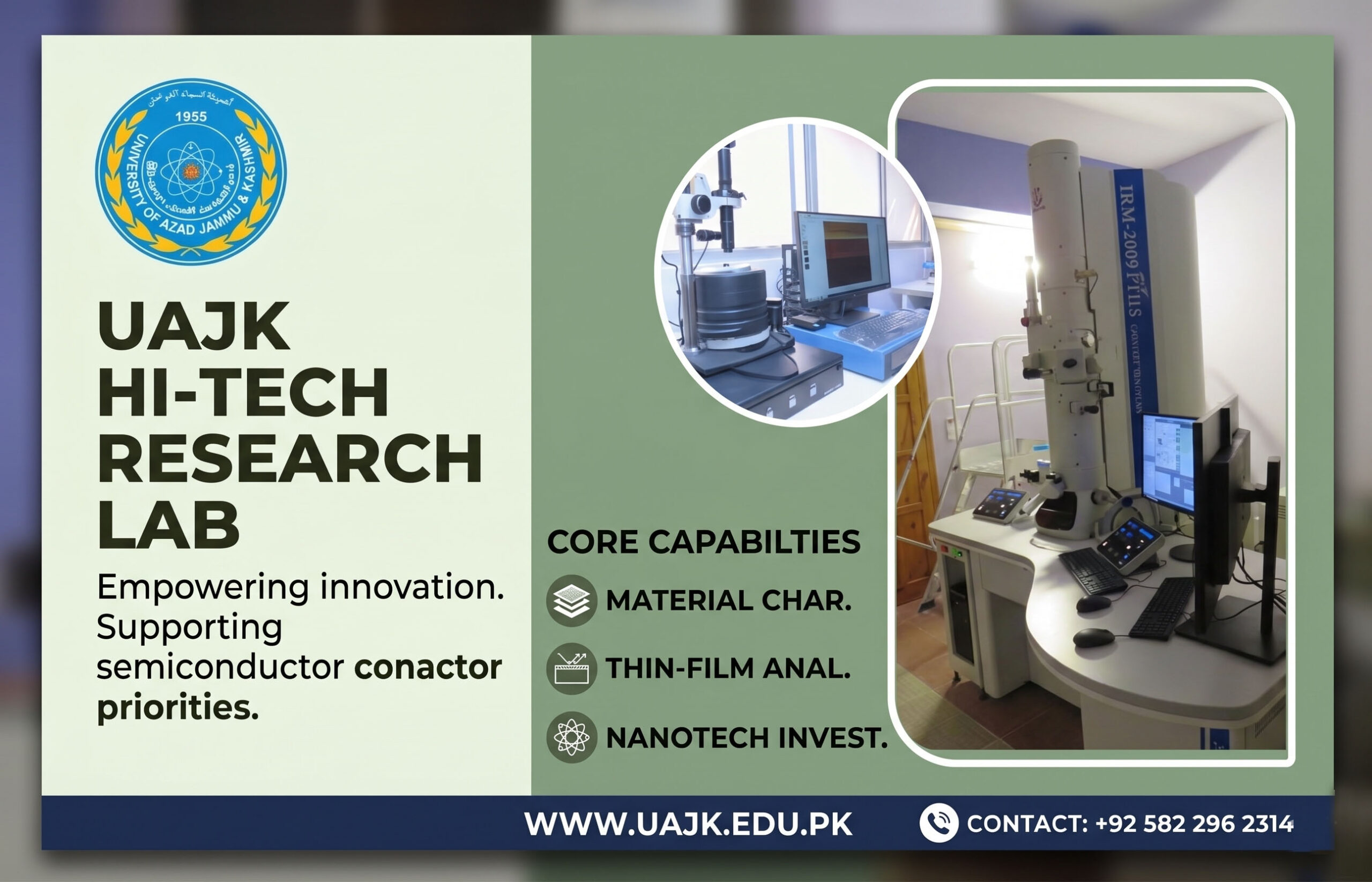
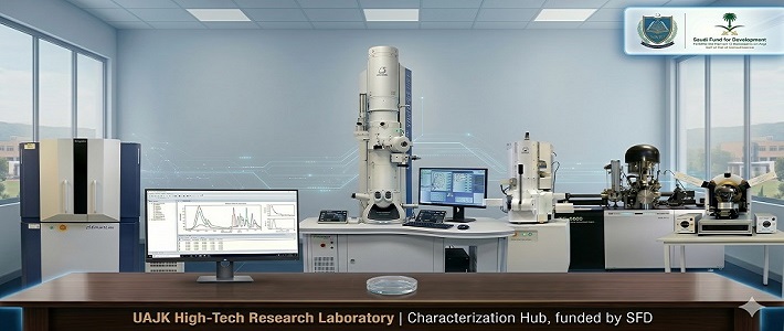
The High-Tech Research Laboratory at the University of Azad Jammu & Kashmir (UAJK) is a state-of-the-art facility dedicated to high-precision material characterization, thin-film analysis, and nano-scale investigations. Supporting cutting-edge research in Materials Science, Nanotechnology, and Applied Physics, the lab serves as a dynamic platform for students, researchers, and professionals.
Established through a Grant-in-Aid Project funded by the Kingdom of Saudi Arabia via the Saudi Fund for Development (SFD), this facility reflects a strategic commitment to enhancing scientific infrastructure and promoting technological advancement in the region.
Our facilities are closely aligned with Pakistan’s National Strategic Priorities in Semiconductor and Microelectronics Development. The laboratory fulfills critical requirements for:
- Research & Prototyping: Supporting microelectronic fabrication processes.
- Workforce Development: Cultivating a skilled workforce to support national technological self-reliance.
- Innovation Culture: Fostering experimentation and applied research.
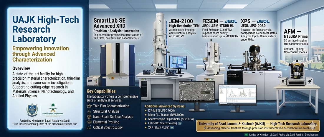
The laboratory offers a comprehensive suite of analytical services:
- Thin Film Characterization: Multi-layer analysis and optical constant (n, k) determination.
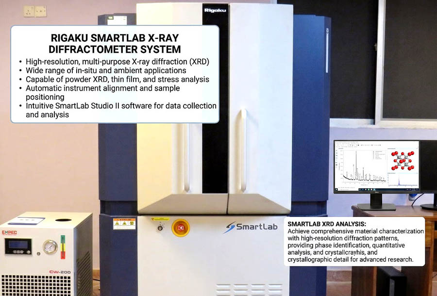
- Structural Analysis: Phase identification and crystal structure determination via XRD.
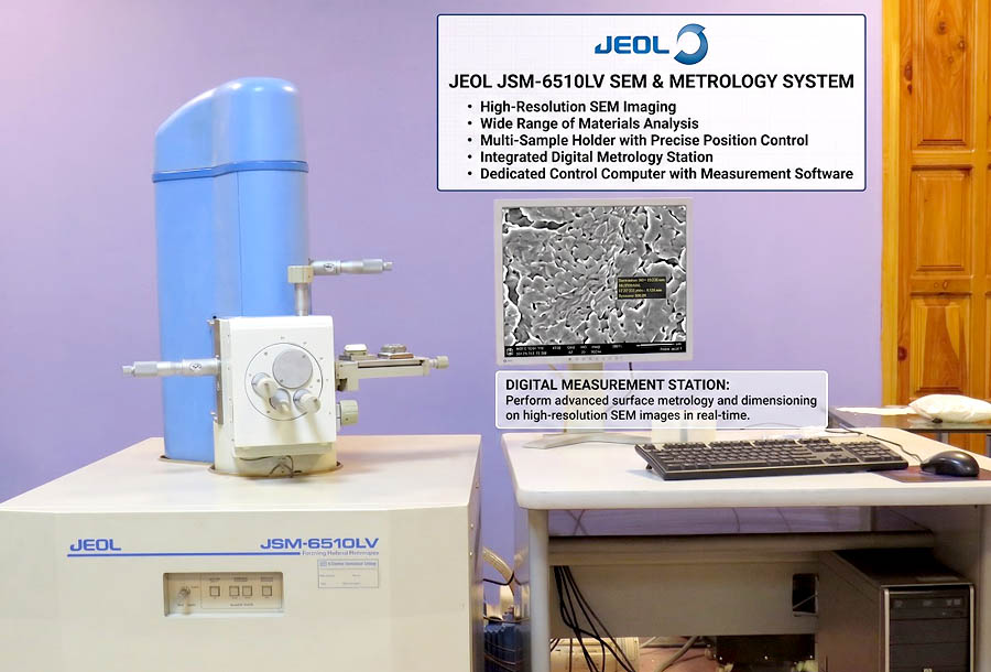
- Nano-Scale Surface Analysis: High-resolution 3D topography and surface potential mapping.
- Elemental Profiling: Ultra-low trace element detection (ICP-MS) and non-destructive XRF analysis.
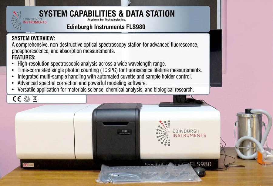
- Optical Spectroscopy: Fluorescence emission studies and band gap evaluation.
Precision • Analysis • Innovation
Purpose: Engineered for precise characterization of thin films, powders, and nanomaterials.
Key Features: Automated alignment, high-speed performance, and modular design.
Specifications: Cu/Mo radiation source, hybrid detector, and integrated analysis software.
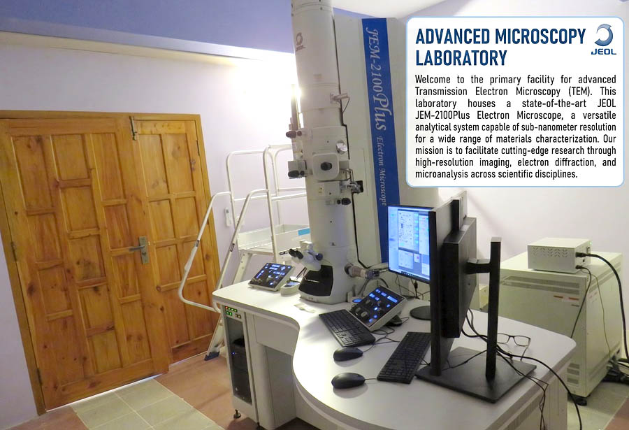
Purpose: Atomic-scale imaging and structural analysis at accelerating voltages up to 200 kV.
Applications: Nanomaterials, semiconductor research, and metallurgy.
Technical Specs: Point resolution of ~0.23 nm with a 19M pixel CMOS camera.
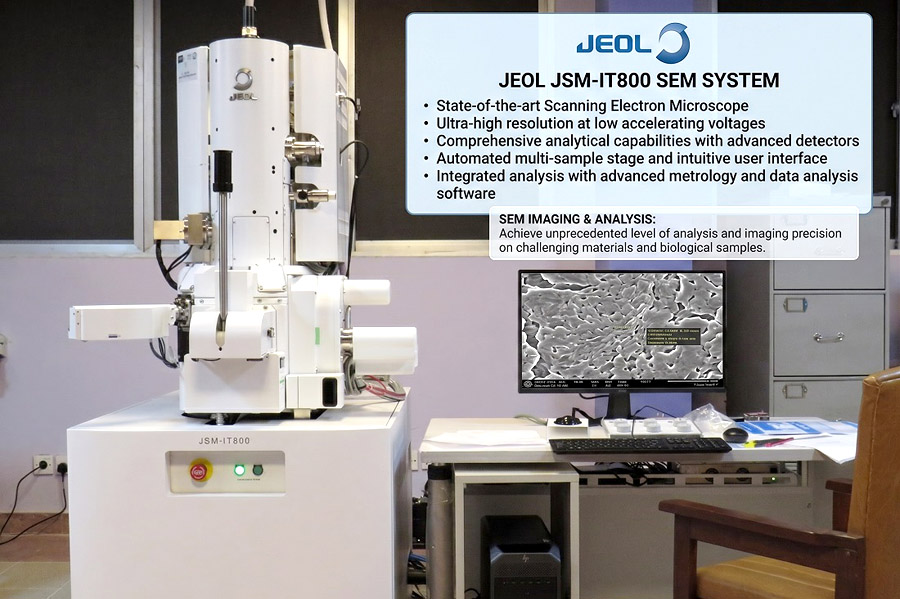
Purpose: Next-generation ultra-high-resolution surface and microstructural analysis.
Highlight: Equipped with a Field Emission Gun (FEG) for superior beam quality even at low voltages.
Capability: Magnification up to ~800,000× with 1 nm resolution.
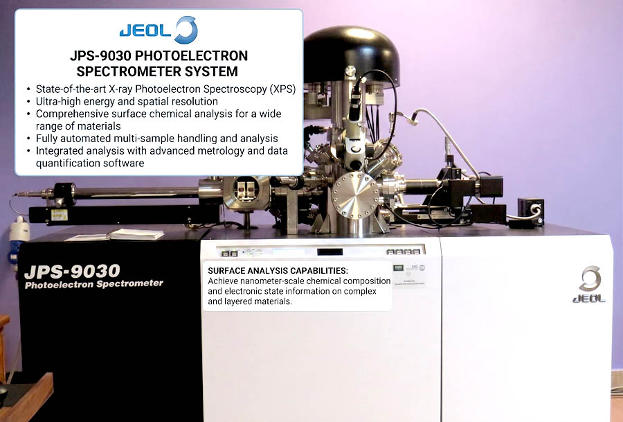
Purpose: Powerful surface analysis to determine elemental composition and chemical states.
Detail: Analyzes the top 1–10 nm of a material surface under ultra-high vacuum (UHV).
Applications: Corrosion studies, catalysts, and thin-film coatings.
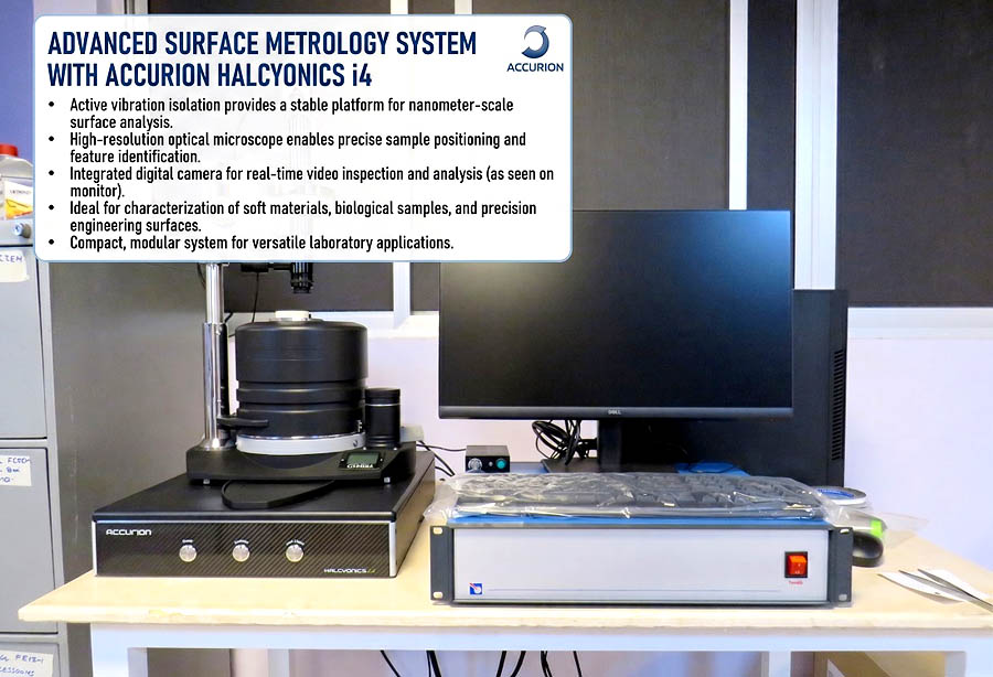
Purpose: 3D surface imaging and mechanical/electrical characterization at the sub-nanometer scale.
Modes: Contact, Tapping, Non-contact, and MFM modes.
Feature: Includes an active vibration isolation system for precision measurements.
The laboratory also features cutting-edge analytical platforms:
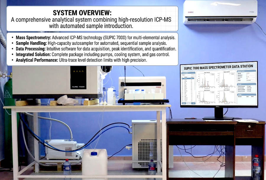
- ICP-MS (SUPEC 7000): Detects trace elements at parts-per-trillion (ppt) levels.
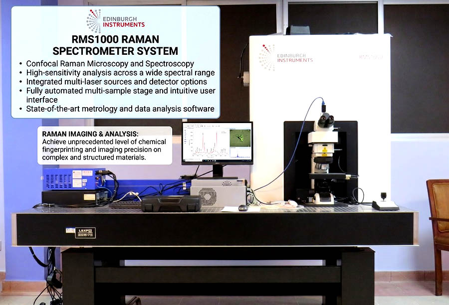
- Micro PL / Raman (RMS1000): Confocal micro-area analysis for chemical and structural characterization.
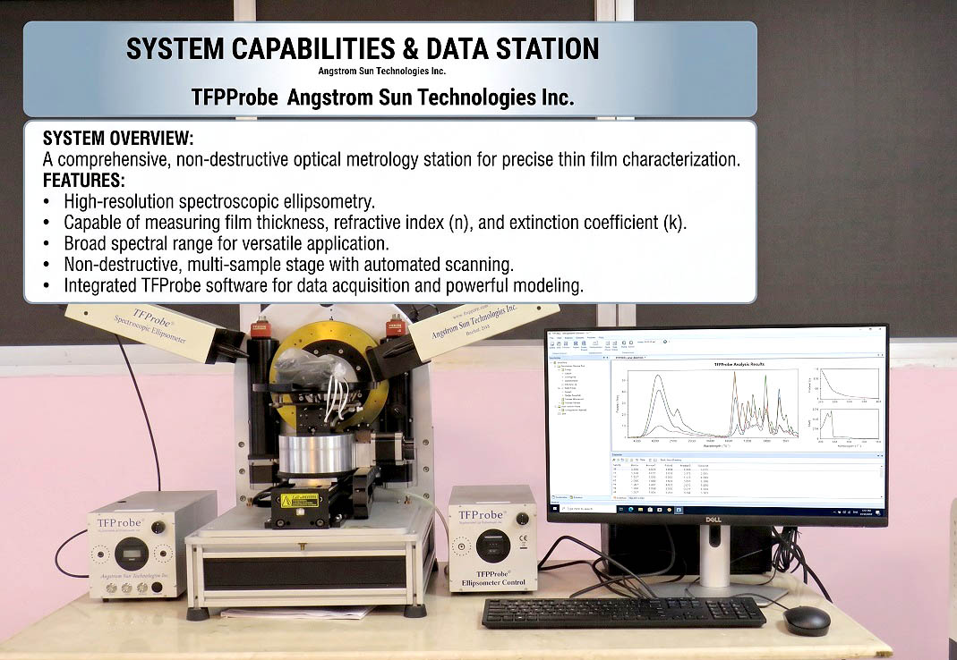
- Spectroscopic Ellipsometer (SE200BA): Non-destructive measurement of thin-film thickness (nm to µm scale).
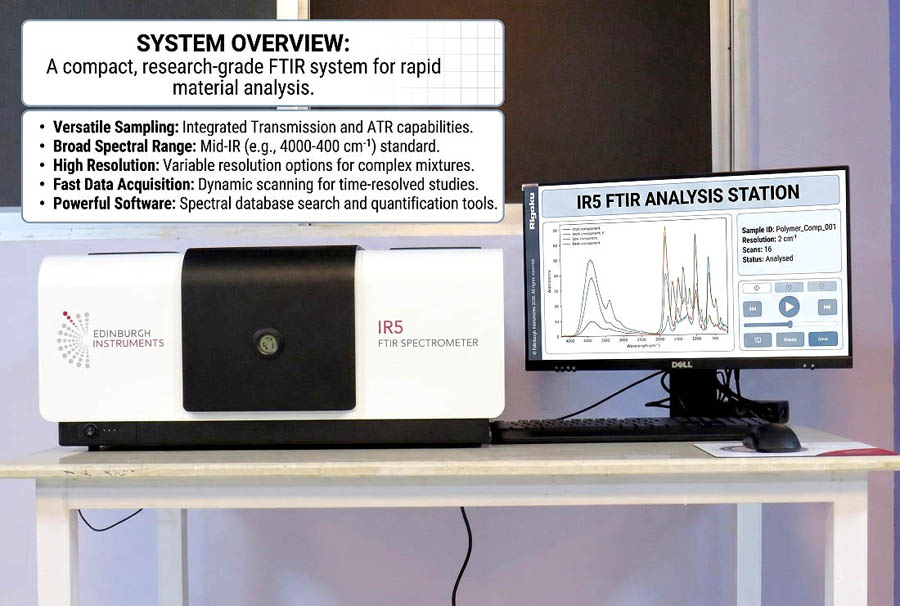
- FTIR (IR5 Spectrometer): Molecular fingerprinting for organic and inorganic substances.
- XRF (ElvaX PLUS): Fast, non-destructive elemental analysis from Na to U.
High-Tech Research Laboratory
King Abdullah Campus
University of Azad Jammu & Kashmir (UAJK)
Muzaffarabad, Azad Jammu and Kashmir, Pakistan
📞 +92 582 296 2314
📧 physics@uajk.edu.pk